UNIVERSAL PULSE GENERATOR
MODEL 6040
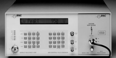
The Model 6040 System consists of a crystal-controlled programmable pulse/digital delay generator mainframe and a family of optional plug-in modules. The 6040 itself generates TTL and ECL outputs at rates to 100MHz with 1 ns or less rise times and a 1 nanosecond resolution for pulse width, delay and double pulse timing.
The interchangeable modules provide the instrument with additional capabilities such as faster transition times, higher pulse amplitudes, and generating optical pulses.
SECTION 1 SPECIFICATIONS 1
GPIB/RS-232 Command List Summary Status Byte Summaries SECTION 2 OPERATING INFORMATIONGeneral
LCD Display LED Annunciator Keypads Plug-In Module Receptacle
RS-232 Connector ECL OUT Connector MODULE DISABLE Jack RESET Button 115 V/ 230 V Selection Switch and Fuse
|
Command Set SECTION 3 THEORY OF OPERATIONGeneral
Software and Microprocessor
Simplified Interconnection Diagram
SECTION 4 MAINTENANCE AND CALIBRATIONCalibration
Equipment Required Procedure | |
| ||
The following warnings, which appear both here and in the main body of the test, are to alert the user of potential safety hazards and to encourage safe operating practices.
| WARNING: To avoid possible electric shock, observe the following. Do not operate with the cover removed. Exposed ac power is present even with the power switch off. Be sure the ground conductor of the ac power cord connects the instrument to a solid earth ground. |
| WARNING: To remove all ac power from the unit the line cord must be unplugged. |
| WARNING: To avoid accidental shock, unplug the line cord and turn the power off before checking or replacing the fuse. For protection against fire, use only the specified fuse value. Do not attempt to bypass or repair the fuse. |
The following cautions, which appear both here and in the main body of the text, are to prevent equipment damage that could result from improper operation.
| CAUTION: The module must be installed with mainframe power off. A module can be damaged or have its memory corrupted if inserted or removed from the mainframe with the power on. |
| CAUTION: Before plugging the instrument into a 234 V ac line, be sure the 115 V/230 V selection switch is set to 230 V and a fuse of proper value is in place. Do not move this switch while the power is on. |
| INTERNAL REP RATE | |||
| Range: | 0.01 Hz - 100 MHz. | ||
| Resolution: | 4 digits. | ||
| Accuracy: | 0.01%. | ||
| DELAY | |||
| Range: | 0 - 640 s. | ||
| Resolution: | 1 ns or 5 digits, whichever is greater. | ||
| Jitter (rms): | 25 ps or 0.01% of Delay, whichever is greater. | ||
| Accuracy: | 0 to 9 ns, 1 ns; 10 ns to 640 s, 0.5 ns or 0.2% of Delay, whichever is greater. | ||
| WIDTH | |||
| Range: | 3 ns - 640 s. | ||
| Resolution: | 1 ns or 5 digits, whichever is greater. | ||
| Jitter (rms): | 25 ps or 0.01% of Width, whichever is greater. | ||
| Accuracy: | 3 ns to 9 ns, 1 ns; 10 ns to 640 s, 0.5 ns or 0.2% of Width, whichever is greater. | ||
| PULSE SPACING | |||
| Minimum Pulse Separation: | For Widths < 160 ns: 5 ns. | ||
| For Widths =< 160 ns: 150 ns. | |||
| Trailing to leading edges. | |||
| Maximum Delay: | For Delays < 160 Ns: Delay (trig. period)- 5 Ns. | ||
| For Delays 160 Ns: Delay (trig. period) - 150Ns. | |||
| (For Double Pulses, see also minimum Pulse Separation.) | |||
| SINGLE CYCLE | Depression of the ENTER or EXEC key will initiate a single delay and width sequence. | ||
| INPUT CHARACTERISTICS | |||
| TRIG IN | External trigger to initiate delay and width sequences. | ||
| Range: | 0 - 100 MHz. | ||
| Input Impedance: | 50 ohms. | ||
| Slope: | |||
| Minimum Pulse Width: | 3 ns. | ||
| Minimum Signal Amplitude: | 100 mV. | ||
| Maximum Signal Amplitude: | ±7 V. | ||
| Threshold Range: | ±2.5 V. | ||
| Threshold Resolution: | 10 mV. | ||
| Trigger Jitter: | 20 ps rms (between TRIG IN and TRIG OUT). | ||
| MODULE DISABLE | Allows the outputs on some modules to be remotely disabled. | ||
| Disable: | 4 V - 5 V, 5 mA sourcing current (into the 6040) or contact opening. | ||
| Enable: | 0 - 300 mV, 5 mA sinking current (from the 6040), contact closure, or plug removed from jack. | ||
| OUTPUT CHARACTERISTICS | |||
| PULSE OUT | Provides the signal selected by the rep rate, delay, width, and single/ double pulse settings. Corresponds in timing to ECL OUT and to module outputs. | ||
| Amplitude: | +5 V into 50 ohms. | ||
| Transition Times: | 1 ns rise time, 1.5 fall time. | ||
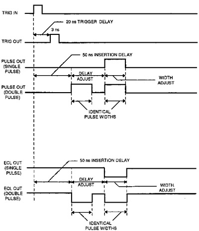
| Insertion Delay: | 50 ns typical (between TRIG IN and PULSE OUT; see Figure 1-1). | ||
| ECL OUT | Provides an ECL version of PULSE OUT. | ||
| Amplitude: | -0.8 V to -1.8 V into 50 ohms ("low true" pulses). | ||
| Transition Times: | 700 ps. | ||
| Insertion Delay | 50 ns typical (between TRIG IN and ECL OUT; see Figure 1-1). | ||
| TRIG OUT | Denotes the start of a timing cycle. | ||
| Amplitude: | +2 V into 50 ohms, +4 V into 100 ohms. | ||
| Transition Times: | 3 ns. | ||
| Pulse Width: | 3 ns. | ||
| Trigger Delay: | 20 ns typical (between TRIG IN and TRIG OUT). | ||
| MODES | With a module installed, four main operating modes are available. The Mode selection is module dependent. | PULS | E|
| Single Pulse: | Conventional pulse generator with rate, delay and width controlled by the 6040 mainframe (see Figure 1-1). | ||
| Double Pulse: | A pair of identical pulses of the selected width with leading edges separated by the selected delay. | ||
| External Drive: | Produces pulses corresponding in rate and duty cycle to an external pulse train. Available with some modules. | ||
| EXTERNAL MODULATION | Converts digital and analog electrical signals into their optical equivalent. | ||
| IMPULSE | |||
| Single Impulse: | A subnanosecond pulse of fixed width and amplitude, with rate and delay conrolled by the 6040 mainframe. | ||
| Double Impulse: | A pair of identical impulses separated by the selected delay. | ||
| CW | Provides a steady-state, adjustable power level. | ||
| PROGRAMMING | |||
| GPIB IEEE-488 | Remote interface with all functions and parameters programmable and bus triggerable. Interface Functions: SHl, AHl, T6, TE0, L4, LE0, SRl, RLl, PP0, DCl, DTl, C0. | ||
| RS-232 | Remote interface with all functions and parameters programmable in full or half-duplex to 1200 baud and bus triggerable. | ||
| LOCAL | Pushbutton manual entry with panel LCD display. | ||
| GENERAL | |||
| DIMENSIONS | 12.75" W x 5.25" H x 16" D (324 mm x 133 mm x 406 mm). | ||
| Rack Mount: | 19" W x 6.97" H x 16" D (483 mm x 177 mm x 406 mm). | ||
| WEIGHT | 16 lbs net (7.3 kg); 23 lbs shipping (10.4 kg). | ||
| Rack Mount: | 5 lbs net (2.3 kg); 10 lbs shipping (4.5 kg). | ||
| POWER | 115/230 V ±10 %, 50/60 Hz, 80 W. | ||
| AMBIENT TEMPERATURE | Operating Range: 0o - 50o C (32o -122o F). Specifications apply: 10o - 40o C (50o - 104o F). | ||
| MODULE CHARACTERICS | |||
| MODULE MEMORY | |||
| PERMANENT MEMORY | A ROM in the module determines the instrument's allowable operating conditions and display units. | ||
| STORE | Ten complete instrument settings can be stored in the module's nonvolatile RAM. The module may be removed without loss of these settings. | ||
| RECALL | Stored settings can be manually recalled or bus transferred to the mainframe. The setting in memory 0 is activated automatically upon power-up or reset. | ||
| DIMENSIONS | 3.75" W x 4.9" H x 10" D (95 mm x 124 mm x 254 mm). | ||
| WEIGHT | 2 lbs net (0.9 kg); 7 lbs shipping (3.2 kg). |
| Category | Command | Description |
| Status: | ES | Error Status |
| IS | Instrument status | |
| PS | Module status | |
| Panel Control: | ||
| MODE: | MO PL | Pulse |
| MO IM | Impulse | |
| MO CW | C.W. | |
| MO EM | External Modulation | |
| TRIGGER: | TR IN {f} | Internal rep-rate generator {set to f Hz} |
| TR ET {v} | External Trigger {threshold set to v volts} | |
| TR EP | External Trigger Slope, positive | |
| TR EN | External Trigger Slope, negative | |
| TR ED {v} | External Drive {threshold set to v volts} | |
| TR SC | Single Cycle | |
| TIMING: | TI DL {t} | Timing Delay {set to t seconds} |
| TI WD {t} | Timing Width {set to t seconds} | |
| TI SP | Single Pulse | |
| TI DP | Double Pulse | |
| LEVEL: | LV PK{x} | Peak {set to x units (V, W, dBm)} |
| LV BL {x} | Baseline {set to x units (V, W, dBm)} | |
| LV AV {x} | CW {set to x units (V, W, dBm)} | |
| LV EM {x} | External Modulation {set to x units (V, W, dBm)} | |
| MEMORY: | ST i | Store instrument setting in memory i (0-9) |
| RE i | Recall instrument setting from memory i (0-9) | |
| FUNCTIONS: | FA | Execute function key A |
| FB | Execute function key B | |
| FC | Execute function key C | |
| SCAN: | LF {i} | Move cursor left (i times) |
| RT {i} | Move cursor right (i times) | |
| UP {i} | Increment digit (i times) | |
| DN {i} | Decrement digit (i times) | |
| Display: | DS ON | Display on |
| DS OFF | Display off | |
| DS ST {c} | Display ASCII string c | |
| Supplemental: | CL | Clear Instrument |
| ; | Suppress activation in hardware | |
| EX | Execute | |
| RL | Reload into hardware |
| Bit | Description |
| 7 | Always zero |
| 6 | Always zero |
| 5 | Always zero |
| 4 | Always zero |
| 3 | Trigger has occurred |
| 2 | Overlap |
| 1 | PLL out of lock |
| 0 | Timing cycle in progress |
| Bit | Description |
| 7 | Always zero |
| 6 | Always zero |
| 5 | Always zero |
| 4 | Always zero |
| 3 | Always zero |
| 2 | Always zero |
| 1 | Overrange |
| 0 | Unrecognized command |
The Module Status byte is module dependent. Refer to the module's instruction
manual.
SECTION 2
OPERATING INFORMATION
GENERAL
POWER UP
When power is first applied, the mainframe performs a test to determine if a module is installed. If a module is present, the limits for each module dependent parameter are transferred to the mainframe. The memory is checked for any errors and the parameters in memory 0 are loaded into the mainframe.
If a module is not present, the parameters are set as indicated in Table 2-1.
| MODE: | Pulse |
| TRIG: | Single Cycle (with other values set as follows) |
| Internal Trigger Rate = 1 kHz | |
| External Trigger Threshold = 0 V | |
| External Trigger Slope: + | |
| TIMING: | Width = 1 s |
| Delay = 1 s | |
| Single Pulse | |
| GPIB/RS-232: | IEEE-488 Address = 6 |
| Baud Rate = 1200 | |
| Full Duplex | |
| Remote Enabled |
When the 6040 is first turned on, the display will show the software version number. If a module is present, the LCD will then momentarily display "MEMORY CHECK," followed by the module I.D. display. Without a module, the display will read "6040 No Plug-In."
Module Installation| CAUTION: The module must be installed with mainframe power off. A module can be damaged or have its memory corrupted if inserted or removed from the mainframe with the power on. |
To install a module, turn the power off, slide the module in and tighten the mount screw knob.
Warm Up RequirementsThe instrument should be allowed to warm up for 30 minutes before high precision mesurements are made. Less critical tests can be performed immediately after turn-on. Please refer to the module's manual to determine if it requires an additional warm up period.
Safety PrecautionsThe safety warnings and cautions that appear in this manual are listed at the end of the table of contents. Some modules have high voltage or laser outputs and additional safety precautions should be taken. See the module manual for details.
| WARNING: To avoid possible electric shock, observe the following. Do not operate with the cover removed. Exposed ac power is present even with the power switch off. Be sure the ground conductor of the ac power cord connects the instrument to a solid earth ground. |
The electrical signal inputs and outputs have fast rise and fall times containing frequency components far in excess of 100 MHz. All signal handling components such as loads, cables, attenuators, connectors and oscilloscopes should have a response exceeding 100 MHz and preferably 350 MHz. Cable and load impedance mismatch will cause signal reflections and result in distorted waveforms and measurement errors. Some sampling oscilloscopes will require attenuators to protect their inputs.
TROUBLESHOOTINGTo start, make sure that the line cord is plugged in all the way, and that the power-on key switch is in the ON position. Verify that the ll5 V/230 V selection switch is properly set for your area. (If it is not, unplug the line cord and move the switch. Make sure the proper fuse in in place before plugging the cord back in.)
With the line cord unplugged check the fuse. Make sure that it has not blown and that it is of the correct value for the line voltage being used.
When ac power is applied, you should be able to hear the fan. The unit will not operate properly if the side vents are blocked.
A thermal cutoff switch will shut off the power to everything but the fan should the temperature exceed 50o C. Power will be restored when the unit has cooled sufficiently. Make sure that the fan and the side vents are not blocked, and that the fan is operating properly.
With the power off, make sure that the module is seated correctly in the mainframe.
LCD ContrastIf there are no characters on the LCD or the contrast is poor, a simple internal adjustment may solve the problem (see the calibration procedure for details).
Cold BootIf the instrument turns on, but is completely unresponsive to the keyboard or displays the error message "Invalid Function," then the module's memory may have been corrupted causing the instrument to "hang up." To correct for this, turn the unit off, then hold down the ENTER key, and turn the power back on. This will initialize the module's memory to its default settings (see the module's manual for the specific values).
Quick TestSince the 6040 uses a modular approach, operating problems can arise from either the mainframe unit or the installed module: the problem must be localized to one or the other. To test the mainframe, turn the power off, remove the module, and switch the power back on. Press the TRIG key until the internal trigger parameter is displayed ("Trig Int: 1.000 kHz"). Press the {1} key, the {10x} key, the {5} key, and the ENTER key in sequence. The display will read "Trg Int: 100.0 kHz."
Connect the TRIG OUT and PULSE OUT to channels A and B of an oscilloscope. Trigger the oscilloscope on the leading edge of TRIG OUT. Set the oscilloscope for 1 æs per division. Display the PULSE OUT. A pulse of +5 V amplitude and 1 æs duration should occur 1 æs into the sweep.
Press the TIMING key to display the Delay parameter ("Delay: 1.000 æs"). Move
the cursor (using the { } key) to underline the 1 æs decade. Now use the
increment key { } to increase the Delay noting that the incidence of PULSE OUT
moves in 1 æs steps. Repeat this with the Width parameter to change the duration
of PULSE OUT.
For quick testing of the module, repeat the above using the module output (an optical detector may be necessary). Since some modules may have rep rate and width limitations, the specific values above may have to be modified, but the general procedure is the same.
GPIB and RS-232 ProblemsFor remote operation from either GPIB or RS-232, the {GPIB/RS-232} key menu must be set to display "Remote Enabled."
When using the GPIB, make sure that the GPIB cable is properly attached and that the address is specified correctly. The default address is 6, but may be set between 1 and 30.
The 6040 will respond to remote commands only if the Remote Enable line (REM) is asserted. When this happens the LCD will display "GPIB Remote Mode," and all keys except LOCAL will be disabled.
The LOCAL key allows the user to return to manual operation (unless the GPIB command LLO has disabled it).
For the RS-232, again check the cable, but also verify that Baud Rate and Duplex are set correctly.
FRONT PANEL DESCRIPTIONThe power switch, located in the lower left corner of the front panel, is keyed to prevent unauthorized use. The key can be removed only when the switch is turned to the off position.
| WARNING: To remove all ac power from the unit, the line cord must be unplugged. |
The 6040 has a 20-character liquid crystal display (LCD). This displays all menus and data while the unit is being programmed from the front panel. In the following descriptions the display for each menu is given.
LED ANNUNCIATORThe front panel has a set of seven LED indicators on the left side of the panel. The upper four LEDs, labeled PULSE, IMPLS (Impulse), CW (Continuous Wave) and MOD (External Modulation), reflect the current Mode setting. This allows continuous monitoring of the Mode setting.
The next two LEDs, labeled TRIG'D (triggered) and OVRLP (overlap), are used to indicate the status of triggering in the Pulse and Impulse Modes. The TRIG'D LED is illuminated if there is a signal present at the front panel TRIG IN jack that exceeds the threshold setting for an external trigger. The OVRLP LED indicates that a potential triggering error exists. It blinks when the combination of rep rate, Width and Delay results in some pulses not being generated. This occurs when the Minimum Pulse Separation and Maximum Delay conditions are not met (see the Specifications section).
Finally, the bottom LED is labeled REM (remote) and indicates that the 6040 is under remote computer control (via GPIB or RS-232).
KEYPADSThe 6040 has two keypads. The left keypad is used to control the operating state (Trigger, Timing, Mode, etc.) and to modify existing parameters (increment/decrement value). The right keypad is used primarlily to enter numeric data for new parameters. It is also used to toggle the states of certain parameters (e.g. Single Pulse/Double Pulse) and to trigger the instrument under Single Cycle operation.
Control KeypadSome of these keys are dependent on the presence of a plug-in module. For example, the LEVEL, STORE and RECALL keys function only with a module installed. The keys on the control keypad can be divided into the following subsets: menu key, memory keys, function keys, and scan keys, as well as the LOCAL and UNITS keys.
The five menu keys, MODE, TRIG, TIMING, LEVEL, and GPIB/RS-232, step through
a number of possible states or parameter displays, allowing the user to
configure the instrument's operating characteristics. The memory keys, STORE and
RECALL, allow storage and retrieval of ten complete instrument settings. The
function keys are reserved for use with future modules. The scan keys, { },
{
},
{ }, {
}, { }, and {
 } are
used to modify parameters that have been previously entered.
} are
used to modify parameters that have been previously entered.
The two remaining keys do not fall into any of the above categories. The LOCAL key returns instrument control to the front panel from either GPIB or RS-232. The UNITS key allows the user to select between different display units for the level parameter (an optical unit, for example, may allow the display of the level settings in units of either Watts or dBm).
Numeric KeypadThe right keypad is similar to a calculator. It has keys for the decimal digits (0-9), the decimal point (.), sign change (), exponent (10x), backspace (BK SPC), enter (ENTER), and execute (EXEC). ENTER and EXEC are used to terminate data entry and also to trigger a Single Cycle timing sequence. The {, SGL/DBL} key is used both to indicate negative values and to toggle between Single Pulse and Double Pulse operation.
CONNECTORSThere are three BNC connectors on the front panel. These are used in the Pulse and Impulse Modes to monitor or trigger the pulse generator.
PULSE OUT provides waveform synchronized to TRIG OUT. The time position (with respect to TRIG OUT) and duration of this output are set by the Delay and Width, respectively. PULSE OUT produces pulses of a fixed +5 V amplitude (into 50 ohms) with 1 ns rise times and an 1.5 ns fall times.
PULSE OUT is nominally coincident with the plug-in module's output. The "module delay" (the fixed time between the mainframe PULSE OUT and the module output) depends on the module being used and is given in the module manual. In Impulse Mode, PULSE OUT has a fixed width of 5 ns (the Width setting has no effect in Impulse Mode).
TRIG IN is the input for external triggers. It has a 50 ohm input impedance,
can take input voltages up to ±:7 V dc or 7 V ac pk, and accepts frequencies up
to 100 MHz.
TRIG OUT is the time marker for the beginning of a timing cycle. TRIG OUT has fixed +3 V amplitude (into 50 ohms), a 3 ns width, and transition times of 3 ns. In External Trigger operation, TRIG OUT will occur 20 ns after the TRIG IN signal.
PLUG-IN MODULE RECEPTACLEThe plug-in module receptacle is on the right side of the front panel, and accepts a single BNC 6040 plug-in module. The receptacle consists of an alignment guide, one 40-pin edge connector, and one ConheX coaxial connector.
The 40-pin edge connector allows the 6040 mainframe to control and communicate with the module and also supplies the power to the module.
The ConheX connector delivers the high speed pulse generator DRIVE signal to the module. This signal is an ECL version of the mainframe's front panel PULSE OUT.
REAR PANEL DESCRIPTIONLocated on the rear panel are the GPIB and RS-232 bus interface connectors, the ECL OUT jack, MODULE DISABLE jack, RESET pushbutton, line voltage selection switch and fuse. There is also a heat sink for the power supply regulators, a line cord receptacle and the cooling fan.
GPIB CONNECTORIn the upper left corner is the connector for interfacing with an IEEE-488 GPIB bus. This allows full control of the unit via a remote controller. All front panel settings can be controlled and any parameter can be read.
RS-232 CONNECTORIn the upper center-left corner is the RS-232 connector. As with the GPIB bus, all front panel settings can be controlled and all parameters read.
ECL OUT CONNECTORThis SMA connector provides an ECL version of the PULSE OUT output. Negative pulses, switching from -0.8 V to -1.8 V (standard ECL "low true" levels) with transition times of 700 ps, are produced nominally coincident with the positive pulses generated from the PULSE OUT jack.
MODULE DISABLE JACKThe MODULE DISABLE jack is used in conjunction with optical plug-in modules. This allows the user to disable the module output from a remote location. The connector is an audio phone jack that is normally closed (grounded). When a phone plug is inserted, the jack leads are opened so a plug with a two conductor cord and a switch can be used for control. Whenever the switch is open, the module output will be disabled.
RESET BUTTONThe RESET pushbutton initiates a power-on sequence. This resets the microprocessor board which in turn resets all hardware to its power-on settings.
115 V/ 230 V SELECTION SWITCH AND FUSEThis switch allows operation on either 117 V ac (U.S.) or 234 V ac (European), as well as giving the fuse value for that line setting (1.5 A 3AG Slo-Blo for 117 V, 0.75 A 3AG Slo-Blo for 234 V). Below this switch are the line cord and fuse receptacles. The switch is factory preset and should not be moved unless a new line voltage is used. Note that a new fuse value is required as well for a new line voltage.
| WARNING: To avoid accidental shock, unplug the line cord and turn the power off before checking or replacing the fuse. For protection against fire, use only the specified fuse value. Do not attempt to bypass or repair the fuse. |
| CAUTION: Before plugging the instrument into a 234 V ac line, be sure the selection switch is set to 230 V and a fuse of proper value is in place. Do not move this switch while the power is on. |
The front panel control of the 6040 has been optimized for ease of use and understanding. The control and modification of the operating Mode, states and parameters are realized by a set of control keys. Some of these keys have a single parameter or state associated with them (such as the STORE key), while others have a menu of selections (for example, the MODE key).
For menu keys, the user can sequence through the selections by successively asserting the given key. A menu item is chosen simply by stopping at that item. So that the user may see what selection is in effect on another key without altering the setting, sequencing is done only on repeated assertions of a key. So, for example, the first time the MODE key is pressed, it will simply display the active Mode. Only when it is pressed a second time (without pressing another key) will it cycle to the next Mode selection.
The MODE and TRIG menu keys change the operating state of the 6040 directly. As the user sequences through the Mode menu, the state of the module's output is modified in accordance with the displayed Mode (Pulse, CW, etc.). Similarly, as the user sequences through the Trigger menu, the Trigger source for the pulse generator is set in accordance with the display (Internal, External, Single Cycle).
The TIMING, LEVEL and GPIB/RS-232 keys simply display parameter values and do not change the operating characteristics unless these parameters are modified. The TIMING key, for example, allows the user to examine the Width, Delay and Single/Double Pulse parameters. Only if the user modifies the displayed setting will the operating state of the machine change.
Each plug-in module has its own set of available menu selections. Electrical modules, for example, do not have a CW option in the Mode menu. Manuals for each module describes the menus and range of parameter values that correspond to the module.
Although the user has access to all the parameters and menu items (for a given module) at all times, their action is Mode dependent. Table 2-2 gives a general chart of the menu keys, showing which menu selections have control in each Mode. An x in the column for a given Mode indicates that a menu selection (or parameter modification) has an effect in that Mode.
Note that modifying a given parameter will only change the current operating state of the machine if the parameter is valid for the current Mode setting. For example, in the CW Mode, the parameters associated with the TRIG (Trigger) and TIMING keys will not affect the current operating state (but they will become valid when the Mode is subsequently set to Pulse). Another example is the LEVEL key. For the Pulse Mode, the External Modulation Level parameter will not affect the module's output. Again, only after setting the Mode to External Modulation will this setting become pertinent.
Modifying ParametersA parameter can be altered by two methods: by entering a totally new number using the numeric keypad or by altering the present value incrementally using the scan keys.
Numeric Data EntryTo enter an entirely new value, simply type in the desired value using the digit, decimal point, sign (where appropriate), and exponent keys, and then use either the EXEC (execute) or ENTER key to terminate the data entry. During the entry of values any errors can be corrected using the BK SPC (backspace) key. If the user decides midstream not to modify the parameter, pressing any menu key will nullify the data entry. If the menu key is the one associated with the given parameter, the parameter will be redisplayed with its previous value.
The method for other parameters is the same as above. The decimal point {.} and exponent {10x} keys, however, are not recognized for parameters such as bus address. Also, for parameters that are not signed, the {±} key is not recognized.
Note that when used to change Delay or Width parameters, the ENTER and EXEC key differ slightly. EXEC terminates the current timing cycle and will turn off a pulse if one is in progress. ENTER allows the current timing cycle to complete but prevents the keyboard from responding to new input until the timing cycle has finished.
If a value is entered that is outside the range of acceptable values, the display will momentarily display "Range Error," after which the original value is redisplayed. Parameter Scanning
The second method of altering a parameter is incremental. First display the
desired parameter. Then choose the desired digit with the cursor using the left
{} and right {}
keys. Once the digit is selected, the increment {} and
decrement {} keys allow the incremental modification of the existing value.
In addition, the value will be multiplied (or divided) by ten if the left (or right) key is pressed when the cursor is located at the most (or least) significant digit. This simulates the verniered tuning and range switch associated with analog pulse generators.
If an attempt is made to scan a parameter outside the range of acceptable values, a display of "Range Error" will remain until the scan key is released, at which time the parameter's value is again displayed.
| Key Hit: | Display: | Comments: |
| {TIMING} | <Delay: 1.2340 ms > | Display previous Delay parameter |
| {} |
<Delay: 2.2340 ms > | Increment Delay |
| {} |
<Delay: 22.340 ms > | Multiply Delay by 10 |
| {} |
<Delay: 223.40 ms > | Multiply Delay by 10 |
| {} |
<Delay: 223.40 ms > | Move cursor right (asserting {} 4 times) |
| {} |
<Delay: 223.39 ms > | Decrement Delay |
| {} |
<Delay: 22.339 ms > | Divide Delay by 10 |
All plug-in modules are equipped with a nonvolatile memory. This allows the user to store ten complete instrument settings. Included in each of these are all the parameter values (whether active or not) for the Mode, Trigger, Timing and Level menus as well as which menu selections are currently in effect. These memories are accessed by the STORE and RECALL keys.
To save the present panel state, press STORE followed by the digit key for the memory location desired. To retrieve a previously saved panel state, press RECALL, followed by the digit key of the desired memory. (Note that the ENTER and EXEC keys are not used.)
The GPIB/RS-232 menu parameters are not accessed or retrieved by STORE and RECALL. Instead, the most recent setting for each selection on the GPIB/RS-232 menu is automatically stored in the module. These go into effect as soon as the instrument is turned on (with the module plugged in).
CONTROL KEY DESCRIPTIONSThe following is a detailed description of each key on the control keypad. The discussion follows the grouping given in the Keypads section. The operation of each key is provided along with the dependence that key may have on the presence of a plug-in module. The display associated with each state of the key's operation is shown.
In the diagrams for the display, the character x denotes a digit, and an asterisk (*) denotes an exponential unit (e.g. æ for micro-, k for kilo-, M for mega-).
For the menu keys, an overall chart, showing which menu selections have control in each Mode, is given in Table 2-2. An x in the column for a given Mode indicates that the menu selection operates in that Mode. Note that not all Modes and not all menu selections apply to each module (the appropriate module manuals provide details on this).
Table 2-3 gives a list of the menu selections available for the 6040 when used as a stand alone instrument (without a module installed).
| MODE Menu | ||||
| Pulse | Impulse | CW | External Modulation | |
| TRIG Menu | ||||
| Single Cycle | x | x | ||
| Internal Trigger (and Rate) | x | x | ||
| External Trigger (and Threshold) | x | x | ||
| External Trigger Slope | x | x | ||
| External Drive (and Threshold) | x | |||
| TIMING Menu | ||||
| Delay | x | |||
| Width | x | x | ||
| Single/Double Pulse | x | x | ||
| LEVEL Menu | ||||
| Peak | x | |||
| Baseline | x | |||
| CW | x | |||
| External Modulation | x | |||
| GPIB/RS-232 Menu | x | x | x | x |
| IEEE-488 Address | x | x | x | x |
| Baud Rate | x | x | x | x |
| Full/Half Duplex | x | x | x | x |
| Remote Enable/Disable | x | x | x | x |
| MODE Menu | Pulse |
| TRIG Menu | Single Cycle |
| Internal Trigger (and Rate) | |
| External Trigger (and Threshold) | |
| External Trigger Slope | |
| TIMING Menu | Delay |
| Width | |
| Single/Double Pulse | |
| LEVEL Menu | (not used) |
| GPIB/RS-232 Menu | IEEE-488 Address |
| Baud Rate | |
| Full/Half Duplex | |
| Remote Enable/Disable |
| {MODE} |
Sequences through the Mode menu and determines the type of output waveform produced. The selections are Pulse, Impulse, CW, and External Modulation. These are all module dependent. With no plug-in module, Mode defaults to Pulse. Pulse Mode provides flat topped pulses from the mainframe outputs (PULSE OUT and ECL OUT) and the module output jacks(s). All of these outputs follow the timing menu settings (adjustable Delay, adjustable pulse Width and Single or Double Pulse). The Level menu controls Peak and Baseline amplitudes for the module output. The mainframe PULSE OUT and ECL OUT output levels are fixed (zero to +5 V and -0.8 V to -1..8 V respectively). The trigger source is selected with the Trigger menu. External Drive (on the Trigger menu) is available in this Mode for certain high-speed modules. This allows the module to be digitally modulated (in some cases at rates exceeding 100 MHz) via a connector on the front panel of the module. The mainframe's PULSE OUT and ECL OUT are disabled in this state of operation. Impulse causes the module to produce a pulse output of a fixed (narrow) width and fixed amplitude. A corresponding pulse (of 5 ns duration) is produced from the mainframe PULSE OUT and ECL OUT jacks. The Delay setting and Single or Double Pulse selection can be made with the Timing menu (Width is inoperative). The Level menu settings have no effect in this Mode. The trigger source is selected with the Trigger menu, but External Drive operation cannot be used. Impulse is not available with all modules. CW causes the module to put out a continuous steady-state level as set by the CW setting on the Level menu. The Trigger and Timing menus have no effect in this Mode. CW is not available with all modules. External Modulation allows the output of the plug-in module to be linearly modulated about the level as set by External Modulation on the Level menu. The modulation input is a connector on the front of the plug-in module. In this Mode, the Trigger and Timing menu settings have no effect. This is not available with all modules. Front Panel Display:
< Mode: Impulse > < Mode: C.W. > < Mode: Ext Mod > |
| {TRIG} |
Sequences through the trigger source and parameter menu. This is used in the Pulse and Impulse Modes. The selections are Internal Trigger, External Trigger (threshold and slope), External Drive, and Single Cycle. With no plug-in module, this is set to Single Cycle at power-on. Internal Trigger selects the internal rep-rate generator as the source of triggers for timing cycles and allows the user to set this rate. External Trigger selects the front panel TRIG IN connector as the source of triggers for timing cycles and allows the setting of the discriminator threshold. External Trigger Slope selects which edge of a TRIG IN pulse will initiate a timing cycle. This setting is toggled using the {±, SGL/DBL} key. External Drive switches the source of the digital drive from the internal DRIVE waveform (coincident with the mainframe's front panel PULSE OUT) to the module's EXTERNAL DRIVE coaxial connector. This also allows the setting of the module external drive discriminator threshold. In External Drive operation, the module output goes to the Peak level when the External Drive input is above the threshold voltage and returns to the Baseline level when the input is below the threshold. Timing menu settings are ignored and mainframe TRIG OUT, PULSE OUT and ECL OUT jacks are disabled. External Drive is only available with certain plug-in modules. Single Cycle causes a timing cycle to be generated once every time the EXEC or ENTER key is pressed. Front Panel Display:
<Trg Ext: x.xx *V > < Trigger Slope: + > or < Trigger Slope: - > < Single Cycle > <Ext Drv: x.xx *V > |
| {TIMING} |
Sequences through the pulse timing parameter menu. This is used in the Pulse and Impulse Modes (but has no effect on External Drive operation). The selections are Delay, Width, and Single/Double Pulse. These are not plug-in module dependent. Delay controls the time interval from the TRIG OUT pulse to the mainframe (PULSE OUT and ECL OUT) or module outputs. In Single Pulse operation, Delay specifies the interval between the leading edge of the TRIG OUT signal and the leading edge of the output pulse or impulse (plus a fixed delay-see Figure 1-1). In Double Pulse operation, Delay determines the leading edge separation between the pair of output pulses or impulses as well as the interval between TRIG OUT and the second of the two pulses or impulses. Width controls the pulse duration of PULSE OUT and ECL OUT (and of the
module output) in Pulse mode. In Impulse Mode, the width is fixed and this
setting has no effect. Single Pulse/Double Pulse determines the number of output pulses or impulses produced for each trigger. In Single Pulse operation, one delayed pulse or impulse is generated for each TRIG OUT pulse. In Double Pulse operation, an initial pulse or impulse is produced at zero Delay as well as a delayed pulse or impulse. The selection of Single or Double Pulse is made with the {±, SGL/DBL} key, which toggles between the two. Front Panel Display:
<Width: x.xxx *s > < Single Pulse > or < Double Pulse > |
| {LEVEL} |
Sequences through the Level parameter menu. The selections are Peak, Baseline, CW, and External Modulation. All of these are plug-in module dependent. With no plug-in module these are not available. Peak Level is used in Pulse Mode. This controls the level of the module output when PULSE OUT is true (or, for External Drive operation, when the EXTERNAL DRIVE input is above the External Drive threshold setting). Baseline Level is the complement of Peak and is also used in Pulse Mode. It controls the module output level when PULSE OUT is false. For some modules this setting is not adjustable, and Baseline is set to zero. External Modulation Level determines the level about which the module output is modulated in the External Modulation Mode. CW Level determines the level of the module output in CW Mode. Front Panel Display (for an optical plug-in module with 3 digit resolution):
< Lv Bsln: x.xx *W > < Lv ExMd: x.xx *W > < Lv C.W.: x.xx *W > |
| {GPIB/RS-232} |
Sequences through the GPIB/RS-232 enable and bus parameters. The selections are IEEE-488 Address, Baud Rate, Full/Half Duplex, and Remote Enable/Disable. These are not plug-in module dependent. IEEE-488 Address determines the listen/talk address of the GPIB. This value can be set to any nonconflicting address between 0 and 30. Baud Rate determines the baud rate for the RS-232. It can be set to 300, 600, 900 or 1200. Full Duplex/Half Duplex determines whether characters will be echoed back through the RS-232. With Full Duplex, each character sent to the 6040 will be echoed back; for Half Duplex no echoing takes place. The selection of full or half is made with the {±, SGL/DBL} key, which toggles between the two. Remote Enable/Remote Disable determines whether the instrument may be operated through the RS-232 or GPIB interface. Remote Enable allows full control of the unit via RS-232/GPIB. Remote Disable only allows the unit to be queried for parameter and Mode settings. The selection of Enable or Disable is made with the {±, SGL/DBL} key, which toggles between the two. Front Panel Display:
< 488 Add: xx > < Bd Rate: xxxx > < Full Duplex > or < Half Duplex > |
These keys allow the storage (retrieval) of a complete panel setting to
(from) the "ith" memory in the module. To store (retrieve) a panel setting,
press STORE (RECALL) followed by the "ith" digit. This causes the immediate
transfer to (from) memory: the ENTER and EXEC keys are not used to terminate
the memory transfer.
| {STORE} | Allows the storage of the present machine state in one of
ten (nonvolatile) memory locations in the module. This is operable only
with a plug-in module installed. Front Panel Display:
< Stored as Set i > |
| {RECALL} | Allows the retrieval of one of ten previously stored
machine states. This is operable only with a plug-in module installed.
Front Panel Display:
< Recalled Set i > |
Scan Keys
} Increments the digit that is underlined by the cursor.
} Decrements the digit that is underlined by the cursor.
} Moves the cursor one digit to the left. If the cursor is at the
most significant digit, the value will be multiplied by ten.}
Moves the cursor one digit to the right. If the cursor is at the least
significant digit, the value will be divided by ten.Function Keys
| {A}, {B}, {C} | These keys are reserved for use with future modules.
< Function A > < Function B > < Function C > |
Miscellaneous Keys
| {UNITS} | Used to select between parameter display units. This is plug-in module dependent. |
| {LOCAL} | Returns control to front panel from either GPIB or RS-232
remote operation. This is not plug-in module dependent.
< LOCAL > |
|
Note: This display appears only on the return to local from remote operation. Also, under GPIB operation, the bus command LLO can disable this key. | |
NUMERIC KEY DESCRIPTIONS
The following is a detailed description of each key on the numeric
keypad.
| {0}...{9} | The digits zero through nine. |
| {.} | The decimal point. |
| {±, SGL/DBL} | Changes the sign of a parameter entered using the digit keys (or of an exponent when pressed after the {10x} key). This key is also used to toggle between positive and negative Trigger Slope, between Single or Double Pulse, between Full or Half Duplex and between Remote Enable and Remote Disable (when the appropriate menu selection appears on the display). |
| {10x} | The exponent key. Digits entered after {10x} has been pressed will be exponents of ten. |
| {BK SPC} | Deletes the last digit entered and moves the cursor one position to the left. The backspace key is only active while data entry is taking place with the numeric keypad. |
| {ENTER} | Terminates data entry from the numeric keypad. When used for entering Delay and Width parameters, ENTER leaves the current timing cycle unaffected, but prevents the keyboard from responding to new input until the timing cycle has completed. This key is also used to manually trigger the instrument under Single Cycle operation. |
| {EXEC} | Terminates data entry from the numeric keypad. When used for entering Delay and Width parameters, EXEC turns off pulses for the remainder of the current timing cycle. This key is also used to manually trigger the instrument under Single Cycle operation. |
REMOTE PROGRAMMING
Remote programming can be accomplished via either the RS-232 serial interface
or the IEEE-488 GPIB. The command sets for the two buses are identical. Commands
sent to the 6040 are case sensitive. Multiple commands, which must be separated
by blanks or commas, may be sent in a single transfer. The command string,
including blanks, cannot exceed 255 characters. Strings, or single commands,
must be terminated with a carriage return. Extra blank spaces are ignored. Error
messages, sent back by the 6040 in response to invalid commands or data, are
listed in Table 2-4.
In all of the commands listed here, i represents an integer value, f, v, and
x may be in integer, floating point, or exponential notation, and c represents
an ASCII character string. Optional parameters are enclosed in curly
brackets.
In general, if optional parameters are omitted then the current value of
those parameters will be sent back (immediately with RS-232 or upon request with
GPIB). Responses sent back from the 6040 (other than error messages) are 20
characters long and correspond to the LCD display that would appear under manual
operation. They are terminated with a carriage return. With GPIB programming,
EOI is asserted with the carriage return.
Command errors are reported in the Error Status Byte. The controller should
verify that the Error Status Byte is zero after each command string is sent: a
zero value indicates no errors have been detected.
The transfer from mainframe memory into hardware of a new parameter can be
suppressed
Table 2-4. GPIB/RS-232 Error Messages
| Primary PCC | Error Message | Meaning |
| XX | "Invalid Comand" | Primary PCC not recognized. |
| MO | "Invalid Mode" | Mode not available for the module type, or secondary PCC not recognized. |
| TR | "Invalid Trigger Command or Data" "Invalid Module Command" "Trigger Range Error" |
Secondary PCC or data not recognized. Trigger choice not available for the module type. Invalid trigger value. |
| TI | "Invalid Timing Command or Data" "Invalid Module Command" "Timing Range Error" |
Secondary PCC or data not recognized. Timing choice not available for the module type. Invalid timing value. |
| LV | "Invalid Level Command or Data" "Invalid Module Command" "Level Range Error" |
Secondary PCC or data not recognized. Level choice not available for the module type. Invalid level value |
| RE, ST | "Memory Range Error" "No Memory Present" |
Invalid or unrecognized memory number. No plug-in module installed. |
| DS | "Invalid Display Command" | Secondary PCC not recognized. |
by following the value with a semicolon. This can be used for loading an
entire front panel state into mainframe memory and saving it in module memory,
without disrupting the current hardware settings. As an example, the string
TR IN 1E3 sets the rep rate generator to 1.000 kHz, whereas the string
TR IN 1E3; does not affect the current setting of the repetition
rate.
INITIAL BUS PARAMETER SELECTION
The {GPIB/RS-232} menu key has a number of items that affect the GPIB and
RS-232 operation.
The Remote Enable/Disable setting determines whether full remote control is
allowed. To allow remote control, select Remote Enable. To prevent remote
control, select Remote Disable. In both cases, the instrument can be queried for
parameter settings and the Mode setting.
Specific to the RS-232 are the Baud Rate and the Full/Half Duplex setting.
These can be set according to the user's needs. Note that Cntrl-Z (ASCII 26)
must be received by the 6040 to enable RS-232 operation. Cntrl-C (ASCII 3)
disables RS-232 operation.
For GPIB operation, the IEEE-488 Addess (listen/talk) should be set to a
unique address so that no bus conflicts arise.
COMMAND SET
The commands are grouped into four sets: status, panel control, display, and
supplemental control commands. The panel control commands have counterparts in
the keypad commands used during front panel programming. The other commands are
unique to remote operation.
Status Commands
The status commands are used to query the status of command transactions, and the state of the mainframe and plug-in module.
| ES | Error Status. This returns a single byte that flags any errors that have occurred since the previous ES command. All bits are set to zero following this instruction. The bit definitions are as follows. | ||||||||||||||||||
Error Status Byte:
Bits 2-7: These bits are always zero and are reserved for future
use. Bit 1: This is set if a parameter was set to a value outside its
allowable boundary. For example, if the command TR IN -5 is sent (set
internal rep-rate generator for -5 Hz), the value would be discarded and
bit 1 would be set. Bit 0: This bit is set if the command is
unrecognized. | |||||||||||||||||||
| IS | Instrument Status. This returns the instrument status
byte. Instrument Status Byte:
Bits 4-7: These bits are always zero and are reserved for future
use. Bit 3: This bit is set if a trigger has occurred that generated a
timing cycle. Bit 2: This bit is set if a trigger has occurred and no timing cycle
has been generated. Bit 1: This bit is set if the PLL for the internal rep rate generator
is unlocked. Bit 0: This bit is set if a timing cycle is in progress.
|
||||||||||||||||||
| PS | Module Status. This returns the module status byte, which is module dependent. For definitions, refer to the module's manual. |
Panel Control Comands (PCCs)
In the Front Panel Programming description, there are a group of keys denoted
as menu keys. They have associated with them a sequence of menu items that allow
the user to select a particular Mode or state of operation or to modify a
specific parameter. The panel control commands (PCCs) are set up in a similar
fashion, except that sequencing is replaced by a second PCC that selects the
specific menu item.
Each front panel menu key has a corresponding PCC. These are the primary
PCCs. Each of these primary PCCs is used in conjunction with a set of secondary
PCCs to select a specific sequenced menu item. There are roughly the same number
of secondary PCCs for a given primary PCC as there are menu items associated
with a similar menu key. This allows the direct selection of Mode, operating
state or parameter via a two instruction command string. Finally, if a parameter
is associated with the primary-secondary PCC command string, the desired value
can be appended to the command string, or, if no value is appended, the present
value of the parameter can be read back by the controller.
The general format for a command string is:
primary PCC {secondary PCC {value x}}
where x is either an integer or floating point value.
There are four primary PCCs, equivalent to the menu keys MODE, TRIG, TIMING,
and LEVEL. These are described in the following. The GPIB/RS-232 key cannot be
controlled remotely.
Mode Control, where the secondary PCC is one of the
following:
If the secondary PCC is omitted, the current Mode setting will be
returned. For example, sending the string MO PL would set the
operating mode to Pulse operation. If the string MO were
subsequently sent, the 20 character string "Mode: Pulse" would be
returned. | |||||||||||||
Trigger Control, where the secondary PCC is one of
the following:
If the value {x} is omitted, the current value is returned. If the
string TR IN 1E3 were sent, the internal rep-rate generator would
be set for a frequency of 1.000 kHz. A subsequent string TR IN
would cause the return of the 20 character string "Trg Int: 1,000
kHz." Once Single Cycle operation has been selected, the 6040 can be
triggered with the EX command (see the Supplemental Control
Commands section). | |||||||||||||
Timing Control, where the secondary PCC is one of
the following:
Width and Delay commands terminate the current timing cycle when
received by the 6040 (just as the EXEC key does under manual
operation). If the value {x} is omitted, the current value is returned. If the
string TI WD 1.23E-3 were sent, the delay would be set for 1.2300
ms. A subsequent string TI DL would cause the return of the 20
character string "Width 1.2300 ms." |
|||||||||||||
Level Control, where the secondary PCC is one of the
following:
If the value {x} is omitted, the current value is returned. If the
string LV PK 1.23E-3 were sent, the peak level would be set to 1.23
mW (for an optical module). A subsequent string LV PK would cause
the return of the 20 character string "Lv Peak: 1.23 mW." The unit used is
dependent on the module. |
There are no secondary PCCs used with the memory commands. The format is
simple: the memory PCC followed by a single integer.
| Recall the panel settings from the "ith" memory,
where i is an integer between and including 0 and 9. The string RE 2 would recall the panel settings in memory 2. | |
| Store the present panel settings in the "ith"
memory, where i is an integer, between and including 0 and
9. The string ST 2 would store the instrument setting in memory 2. |
The following commands control the function keys (reserved for future
use).
| Execute function key A. | |
| Execute function key B. | |
| Execute function key C. |
The last four PCCs operate identically to the four scan keys ( {},
{}, {}, {} ).
When followed by an integer i the commands are equivalent to pressing the
corresponding scan key i times.
| Move the cursor one digit (or i digits) to the left.
| |
| Move the cursor one digit (or i digits) to the right.
| |
| Increment (i times) the digit at the cursor. | |
| Decrement (i times) the digit at the
cursor. |
Display Commands
The display commands allow the user to control the LCD readout from the
GPIB/RS-232 bus. They have no other effect on the operation of the 6040.
| This command causes the response from the 6040 to a
parameter query to be displayed on the LCD. | |
| This returns the instrument to the default state, in which
queried parameters are not displayed on the LCD. The 6040 is always in
this state following power up. | |
| Displays the string c on the LCD, where c consists of up to
20 ASCII characters. |
Supplemental Control Commands
These commands provide additional methods for controlling the instrument.
They do not directly correspond to the keys on the 6040 front panel.
| Clear Instrument. This command recalls the settings
in module memory zero if a module is installed (equivalent to RE
O). With no module installed, the mainframe is set for Single Cycle
triggering (and no other parameters are changed). | |
| The semicolon is used to suppress the loading of parameters
into hardware. When added to the end of a panel control command, that
command is temporarily stored in mainframe memory (not to be confused with
the module memory accessed by STORE and RECALL), but not put into
effect. The command can be activated later in a number of ways. It can be activated by immediately following it with an EX command or by querying that menu item some time later and then immediately following that with EX. For example, either the sequence TR IN 1234; EX or TR IN 1234;...[other commands]...TR IN EX will put 1.234 kHz Internal Triggering into effect. Additionally, a complete set of instrument parameter can be held in mainframe memory using ; repeatedly. These could be activated in hardware as a group with the RL> command or they could be stored in module memory (using the ST i command) and recalled as a group when needed (using RE i). | |
| Execute. This command activates parameters into hardware
and initiates Single Cycle triggers. Under Single Cycle operation,
EX triggers the instrument, causing the pulse of specified Width
and Delay to be produced. If the most recent command received by the 6040
was a parameter query (a panel control command with the argument omitted)
or a command terminated by a semicolon (to load into temporary memory but
not activate a parameter), then EX activates the menu parameter
just queried about or the parameter just loaded into memory. (In this
case, if the instrument is in Single Cycle operation, a trigger is not
produced.) For example, both the command sequences TR IN EX and
TR IN 2E3; EX select Internal Trigger operation. The second also
changes the rep rate to 2 kHz. | |
| Reload. The RL command loads the complete set of instrument parameters from temporary mainframe memory into hardware (see ;). |
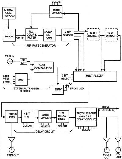
Figure 3-1 shows a simplified block diagram of the timing circuits. There are four main functional groupings: Rep-Rate Generator, External Trigger Circuit, Delay Circuit and Width Circuit. A high speed multiplexer selects either the output of the External Trigger Circuit or one of the frequencies available from the Rep Rate Generator. The selected signal generates a TRIG OUT pulse and triggers the Delay Circuit which in turn triggers the Width Circuit. The result is an output pulse whose delay and width are digitally programmable with 1 ns resolution. The entire signal path from either circuits involves approximately 20 IC gates. Excellent time coherence (~25 ps rms) is advanced through careful layout and the use of high speed ECL devices.
The top rows of blocks represent a frequency synthesizer employing a phase locked loop (PLL) to insure that crystal accuracy is maintained for all rep rates. The dashes (blocks) indicate CMOS counters that are located on the Microprocessor board. By programming the 16-bit divider in the PLL feedback path as well as the 4-bit and two 16-bit dividers outside the loop, all of the required frequencies are obtained.
When the External Trigger Circuit is used, the multiplexer selects the line from the fast comparator. The x2 attenuator at the input provides a wideband low VSWR termination for the external triggers. An 8-bit DAC plus a polarity bit provides 0.2% resolution (20 mV/step) for the trigger threshold level. When solid triggering occurs, an LED indicator lights.
The two remaining circuits (Delay and Width) are essentially identical. An input pulse starts a 100 MHz oscillator running. The 4-bit (ö16) counter begins to count the oscillator pulses. When the programmed Width is reached, the trailing edge of the (previously started) output pulse returns to ground and the entire cycle can be repeated almost immediately. DRIVE, an ECL version of the PULSE OUT output is sent to the plug-in module.
SOFTWARE AND MICROPROCESSOR
The Model 6040 is based on the Intel 80C31 family of microprocessors (see Figure 3-2). This microprocessor, optimized for imbedded controller applications such as the BNC 6040, is very efficient at bit control, has a built-in serial I/O and baud rate control, and supports a six-level interrupt system.
Programs developed for the 6040 are written in the C language using a cross-assembler. Some low level routines are coded in assembly for speed and efficiency.
The software has a timer interrupt for the keypad interface, as well as interrupt driven GPIB and RS-232 routines. The timer interrupt occurs at intervals of 50 ms. This allows optimal keypad detection while minimizing interruptions of other software tasks.
When power is first applied the software determines if a plug-in module is
present and configures the front panel user interface as necessary. This
includes enabling or disabling the selection of certain parameters, Modes, and
Timing states, and the limiting of parameters to boundaries as specified by the
module.
The microprocessor has 64K bytes of code memory, and a separate 64K bytes of
data memory. Code is accessed when the CODE SELECT line (PSEN) is asserted. In
the 6040, the hardware control is realized by "memory mapping" the interface ICs
into the data memory space.
The microprocessor has 8K bytes of RAM which is used for temporary values and
the stack.
The module is mapped into 8K bytes of memory. There is a special bus
interface designed to minimize bus induced noise in the module.
The CMOS timers are mapped into a 2K byte segment of memory. There are a
total of four LSI counters, each having three 16-bit timers, for a total of 12
timers. These are used to augment the range of the ECL circuitry, and interface
via the 20-pin connector, J9.
The ECL I/O is mapped into a 512-byte segment of memory. This allows 32 bits
to control circuitry, and four bits to monitor the timing hardware. These
interface to the timing board via the 40-pin connector, J6.
The front panel control is mapped into a 256-byte segment. This controls the
LCD, scans the keypads (at 50 ms intervals), and drives the LED
annunciators.
The GPIB controller is also mapped into a 256-byte segment. This notifies
(interrupts) the processor when the 6040 has been addressed (as set by the GPIB
key parameter, 488 Add) via the GPIB.
The RS-232 takes advantage of he 80C31's internal serial port. The processor's circuitry interrupts the processor when the RS-232 port is active.
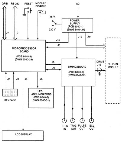
CIRCUIT DESCRIPTIONThis diagram depicts the signal flow between circuit boards in the 6040, as well as inputs and outputs to and from the front panel, rear panel and plug-in module. The printed circuit boards are shown with their assigned number, such as PCB 6040-1 for the Power Supply Board. The schematic number for each board is also shown.
TIMING BOARD (Schematic 6040-32)
Rep-Rate Generator and External Trigger Circuit (Schematic 6040-32,
Sheet 1)
The rep-rate generator schematic consists of Z1, Z2 and Z5. Z8 buffers the
signal from Z5 and drives Z14 (a binary divider) and Z15 (a multiplexer). The
external trigger circuit also supplies a signal to the multiplexer.
The external trigger circuit consists of Z4, Z7, Z13, Z22 and Q3. Z4 (a DAC) is supplied data from the microprocessor board and with the aid of Z7 sets the input trigger level. Q3 when
activated inverts the level polarity. Z13 is a high speed comparator and is
used as the input sensing device. Three sections of Z22 are used to select the
slope of the incoming signal.
The fourth section of Z22 is used to detect the presence of a successful
input trigger, lengthen the pulse (if necessary) and flash the trigger
indicator.
Z8-3 is used to lock out a signal from Z15 and thus prevent triggering of the
6040 when required. The upper portion of Z23 is used to shorten (typically 3 ns)
any pulse on its clock input for timing purposes. Z30-4 is used to stretch the
pulse for use by the CMOS circuits on the microprocessor board.
Delay Circuit. (Schematic 6040-32, Sheet 2)
The delay trigger from sheet 1 starts the delay cycle when Z25 is enabled.
Z25 pin 10 is the trigger input, and pin 11 is a disable from the CMOS circuitry
that prevents additional triggers while the CMOS circuitry is being loaded with
data. The input on pin 9 performs a similar function until coincidence is
reached (the end of the delay cycle).
Z16-15 is a delay line oscillator that runs at 100 MHz and is enabled by
Z18-14. When Z18-12 is set by Z25 the oscillator is enabled and supplies clock
pulses to Z18-11 and Z6 (a binary counter) until both CMOS and ECL coincidence
are present at the same time. When this condition is met there is one more clock
pulse which loads the counter, returns Z18 to its original state and disables
the oscillator.
Z25-7 is used to provide two signals: one to the TRIG OUT amplifier and the
other to the width circuit at the beginning of delay in the Double Pulse mode
only. The Z18-14 output in addition to controlling the oscillator, also provides
a signal to the 1 ns delay circuit (Z9 and Z17). Z17 determines the 0 to 1 ns
increments.
Z9 determines the 2,4,6 or 8 ns delay as selected by Z10. The output of Z10
is buffered and inverted by Z17-15 and the trailing edge of the delay pulse is
detected by Z18-6 which then generates a short pulse ( 3 ns typical). This pulse
is the trigger for the width circuit. Z27 is used to detect the presence of a
trigger during a cycle and fire the overlap indicator via the microprocessor
board.
Width Circuit (Schematic 6040-32, Sheet 3)
The width trigger is inverted by Z26 (when enabled) and sets Z28 starting the
width timing cycle Z26-10 disables the gate when data is being loaded into the
CMOS circuits. Z26-11 disables the gate when a trigger signal sets Z28 and
prevents the acceptance of any additional triggers until the width timing cycle
is completed.
When set by the trigger the Z28-3 output enables the 100 MHz delay line
oscillator (Z31-15). The output of Z31 drives both Z28 and Z32 (a binary
counter) with clock pulses. The carry output of Z32 supplies the CMOS circuits
with clock pulses via Z29-2 and Z11-13. Z32 continues to count until both CMOS
and ECL coincidence is reached. The next clock pulse returns Z28 to its original
state. In addition, this extra clock pulse reloads data into Z32.
At the start of the width timing cycle Z6-15 transmits a rising edge to the clock input of Z28 via DL2. This initiates the width output. The electrical length of DL2 is equivalent to the sum of the propagation time through Z19, Z20, Z21 and Z29 when the data set in the l ns decade is zero. At the end of the width timing cycle, Z26 transmits this edge through the 1 ns circuits (Z19 and Z20), the multiplexer (Z21) and the pulse shaper (Z29-14) to Z28-12 to end the width cycle. The outputs of Z28 supply both the plug-in and the output amplifier with a width signal.
MICROPROCESSOR BOARD (Schematic 6040-33)
CPU and Interface (Schematic 6040-33, Sheet 1)
Z8, is an Intel 80C31 Microprocessor. Since it has no internal program
memory, all program memory is contained in an external EPROM. The output of Z11,
a 10 MHz crystal oscillator (described later), is buffered by Z13C and drives
Z8-19. It also drives the CMOS counter circuits.
Port 0 on Z8 is used as both a bi-directional data bus and lower bit address
latch control. The bi-directional data buffer Z14, points away from the
microprocessor except during a data or I/O read.
Port 0 is also connected to Z15, an 8-bit latch used for demultiplexing
AD0-AD7. The lower eight bits of the address are always placed on the bus during
the first portion of an external memory read or write cycle. Latching of the
address bits occurs when ALE (Address Latch Enable) on Z8-30 (on its trailing
edge) goes from high to low. Also during this first cycle A8-A15 are presented
to an output buffer for the upper eight address lines.
External 4.7 k pull-up resistors are required on the P0 port. Note that the
buffered DATA bus actually contains the both the multiplexed address and data
information though only the data is recovered by other chips on the logic board.
The special "quiet bus", however, re-decodes the multiplexed address/data bus.
This is discussed in greater detail in the Module Interface description (sheet
9).
An internal serial port for communication to a three-wire DCE device is
provided via the CMOS to RS-232C translation devices. Z3 and Z5 are the RS-232C
bus driver and receiver. Note that Z3 is the only device requiring -12 V and +12
V. This is necessary to produce the proper voltage swing for the RS-232C
standard. Baud rates of 300-1200 are supported, and data is fixed at eight bits,
no parity.
Bus and External Memory Control Lines:
Memory is divided into two sections identified as Code and Data. Hardware I/O
is mapped in the Data space.
Code (program memory as opposed to data memory) is read by the microcomputer
when PSEN*, Z8-29, goes low (true). This signal, combined with A0-A15, allows
216 or 65,536 directly addressable program memory locations. Program memory is
stored in Z17 (sheet 2).
Data (Read/Write memory or RAM) is read and latched by the microprocessor
when RD*, Z8-17, goes from low (true) to high (false). While the microprocessor
can theoretically address 65,536 data spaces, only 8192 locations (8K) are used
for the RAM.
I/O (hardware used to control or sense the 6040) is also mapped into the Data
space. This includes the module and timing board control circuits.
Memory and I/O Decoding (Schematic 6040-33, Sheet 2)
Program Memory - ROM:
Z17, the EPROM, encompasses the full 64K code space. During a program code
fetch instruction, PSEN* will cause the internal output buffer of the EPROM to
be placed on the data bus. The internal output buffer is enabled when OE*,
Z17-22, goes low (at the same time Z14 will momentarily point inward, permitting
the data to be transferred into the microprocessor).
RAM and Memory Mapped I/O:
Z25, a decoder, divides the 64K data memory space into eight 8K sections. Y0
selects the RAM (Z24), Y6 selects the plug-in module, and Y7 selects the 8K
allotted for other memory mapped hardware I/O.
Data Memory - RAM:
Read/write data memory or RAM is stored in Z24, a 6264 8K by 8 static RAM. It
contains the current operating parameters and other software variables.
Timer and I/O Decoding (Schematic 6040-33, Sheet 3)
Hardware I/O Data Space:
I/O control, selected by Z25-7 (sheet 2), is realized by mapping all hardware
into the memory space E000 to FFFF. Selections of specific hardware within this
area (such as the 82C54 timers and 82C55 parallel I/O chips) is done by Z35,
another decoder.
The first four chip selects (CS0-CS3) go to the 82C54 timers, CS4 selects Z33
(front panel control), CS5 and CS6 select the ECL timing board interface, and
CS7 selects the GPIB interface.
CMOS Counters:
The four 82C54 counter timer chips (Z16, Z20, Z23, Z27) each contain three
16-bit timers that can generate four independent time delays. The logic
connected to the clocks, gates and outputs of these 12 timers are shown on
schematic sheets 6, 7, and 10. Sheet 3 shows only the microprocessor
interfacing.
Front Panel Interface (Schematic 6040-33, Sheet 4)
Z33 is an 82C55 Parallel Peripheral Interface device with three programmable
8-bit input/output ports. Z33 is selected by CS4 from Z13 (on sheet 3).
Keypad Decoding:
Port A outputs the keyboard scan pattern to the two 4-bit wide columns in the
keypad matrix. The four rows on the 8 x 4 keypad map are input on the lower four
bits on port C. Key decoding works as follows.
Software normally sets port A to all zeroes. During the primary 50 ms
operating system timer tick interrupt, the lower half of port C is tested to see
if any bits are low. A bit will be low if any key is pressed because the 4.7 k
row resistor is pulled low by a connection through the keypad switch.
Once a key is pressed, software selectively scans through the columns one by one testing until the unique combination of a row and column is identified.
LED and LCD Display Interface:
Port B of Z33 is connected to both the data bus of the LCD display and Z30 an
octal latch and port driver for the eight LED's. Strobing of data to control the
LED's is accomplished by bit 4 on Port C. Strobing of data to control the LCD is
by strobing bits 5, 6, and 7 of this same port.
ECL Interface
(Schematic 6040-33, Sheet 5)
The microprocessor uses a pair of 82C55 Programmable Peripheral Interfaces
(PPIs) to control the timing board (PCB 6040-2). The PPIs, Z19 and Z22, control
the timing board via the 40-pin connector J6. Each PPI has three I/O ports which
are one byte wide. All of the ports are for output control except Z22, port C's
lower four bits.
Z19 controls the 1 ns and 10 ns timing decades. Port A controls the delay,
while port B controls the width. Port C is used for resetting the CMOS counters
and to reset the overlap detector on the timing board.
Z22 controls the trigger circuits, enables the CMOS Timing counters, and
monitors the status of hardware on the Timing board. Port A has the SEL A,B, and
C lines, that are used in the rep-rate generator. FRQEN, RALMT, and DBLPLS
enable the trigger generator, the rate limit circuitry, and allow double pulses.
TRGSL and TRGPOL determine the slope and polarity for the External Trigger
circuitry. Port B sets the External Trigger threshold DAC. The lower four bits
of port C allows the microprocessor to monitor when a timing cycle is in
progress (DWPROG), if the PLL is out of lock (PLLK), if a timing cycle error has
occurred (OVRLAP), and if an external trigger has been recognized by the
discriminator (TGR'D). Port C's upper four bits is used to enable the CMOS
timing count chain.
CMOS Delay Circuit (Schematic 6040-33, Sheet 6)
This circuit augments the high speed ECL delay circuitry. It extends the delay from 159 ns to more than 100 s. This is done by utilizing a single LSI counter and four SSI ICs.
Z16 contains three user configurable 16-bit counters, configured as two
programmable counters and a fixed prescaler. The CMOS count can be up to four
bytes wide. The Z16-A counter is loaded with two least significant bytes and is
clocked from the DTTLCK signal, at a frequency of 6.25 MHz (a period of 160
ns).
The Z16-B counter is loaded with the remaining two high order bytes and is
clocked by the output of the prescaler, Z16-C. The prescaler divides the 6.25
MHz DTTLCK signal by 65536 (2 to the 16) producing a frequency of 95.367 Hz.
The presettable counters, Z16-A and Z16-B, are enabled by the signals, DCNT24
and DCNT220, respectively. These come from port C of the PPI Z22. They are set
by the microprocessor according to the Delay setting.
The LDCLK signal is used when the counters are loaded with a new value. This
comes from port C of the PPI, Z22.
The DHLDOFF signal is used to prevent the ECL delay circuitry from initiating
a new delay cycle during the reloading of Z16 at the end of a delay cycle.
The DTTLEN signal allows the ECL circuitry to generate the DTTLCK signal.
The DTTLCOIN signal indicates that the CMOS count chain has reached 0
(counted down).
CMOS Width Circuit (Schematic 6040-33, Sheet 7)
The width counter circuitry is essentially identical to the description of
the delay counters.
The CMOS width circuit is similar to the delay circuit. In the width circuitry Z20 is the LSI counter, and signals that began with a 'D' begin with a 'W'.
Z20 is a 82C54 that contains three user configurable 16-bit counters. These
are configured as two programmable counters, and a fixed prescaler. The CMOS
count can be up to four bytes wide. The Z20-A counter is loaded with two least
significant bytes and is clocked from the WTTLCK signal, at a frequency of 6.25
MHz (a period of 160 ns).
The Z20-B counter is loaded with the remaining two high order bytes and is
clocked by the output of the prescaler Z20-C. The prescaler divides the 6.25 MHz
WTTLCK signal by 65536 (2 16) producing a frequency of 95.367 Hz.
The presettable counters, Z20-A and Z20-B, are enabled by the signals, WCNT24
and WCNT220, respectively. These come from port C of the PPI Z22 and are set by
the microprocessor according to the Width setting.
The LWCLK signal is used when the counters are loaded with a new value from
port C of the PPI Z22.
The WHLWOFF signal is used to prevent the ECL width circuitry from initiating
a new width cycle during the reloading of Z20 at the end of a width cycle.
The WTTLEN signal allows the ECL circuitry to generate the WTTLCK signal.
The WTTLCOIN signal indicates that the CMOS count chain has reached 0
(counted down).
GPIB Interface (Schematic 6040-33, Sheet 8)
Z35's CS7 (chip select 7) enters Z4 on pin 3 and in conjunction with A0-A3
select internal registers on the TMS9914 bus controller. The RD* must be
inverted to accommodate the unusual positive-true DBIN (data bus in) signal.
Z6 is used to divide the 10 MHz logic board oscillator which is output to
Z4's clock input.
Z1 and Z2 are standard 75161 and 75160 interface driver chips normally used
with the 9914. They go to the 26-pin connector which in turn is connected to the
24-pin GPIB connector mounted on the back of the 6040.
Module Interface (Schematic 6040-33, Sheet 9)
The quiet bus, J8, is a specially designed bus to minimize interference
caused by normal CPU bus noise. J8 provides the communication path to the
plug-in modules. (See Table 3-1.)
The microprocessor controls the plug-in module via the 40-pin connector, J8.
There are four interface control lines QRD, QWR, QALE, PLUGIN. QRD and QWR are
used to control the direction of data (read from or write to the module). QALE
is used for demultiplexing the QAD multiplexed data/address lines. PLUGIN
enables the module data transaction.
The data/address bus consists of five address lines and eight multiplexed
data/address lines. This allows an access of 8K bytes of memory or I/O in the
module.
The power for the module is also supplied via J8, but the cable is cut and
fitted with a second 16-pin DIP connector which is routed to the power supply
(PCB 6040-1).
PLL and Rate Limiter (Schematic 6040-33, Sheet 10)
The 20-pin connector, J9, is used for all dynamic signals between the
microprocessor board (PCB 6040-3) and the timing board (PCB 6040-2). (See Table
3-2.)
Table 3-1 J8, Microprocessor to Module Interface Signals
| Signal(s) | Pin Number | Description |
| QAD0-QAD7 | 8-1 | 8 multiplexed data/address lines |
| QA8-QA12 | 16-12 | 5 address lines |
| QRD | 11 | Module read |
| QWR | 10 | Module write |
| QALE | 9 | Address Latch Enable (demux QAD0-QADO7) |
| PLUGIN | 18 | Enables Module interface circuits |
| RESET | 17 | System reset |
| MOD DIS | 19 | Disables Module |
| +5 | 26, 28 | +5 V supply |
| -5.2 V | 34, 36 | -5.2 V supply |
| +12 V | 37, 39 | 12 V supply |
| -12 V | 38, 40 | -12 V supply |
| THE | 27 | +3 V supply |
| GND | 35, 29-33 | Ground |
| 20-25 | Unused |
PLL Synthesizer:
The 6040's internal trigger generator is made of two subsections. The VCO,
loop filters, and range selection circuits are located on the timing board (PCB
6040-2). The 82C54 CMOS dividers are located on the microprocessor board (PCB
6040-3).
Table 3-2. J9, Microprocessor to ECL Interface Signals
| PLLVAR | 14 | PLL variable frequency |
| FTTL1 | 16 | Output of first CMOS frequency divider |
| FTTL2 | 17 | Output of second CMOS frequency divider |
| PLLIN | 15 | VCO input |
| PLLREF | 20 | PLL reference frequency |
| RTLMTTR | 19 | Rate Limit trigger |
| RLMTHD | 18 | Rate Limit Hold signal |
| ELDCLK | 1 | ECL Timing count chain, load clock |
| ELDEN | 3 | ECL Timing count chain, enable load |
| DTTLCK | 7 | Delay time base |
| DHLDOFF | 9 | Disables triggering of ECL Delay |
| DTTLEN | 4 | Enables ECL Delay to generate DTTLCK |
| DTTLCOIN | 10 | CMOS Delay count is at zero |
| WTTLCK | 5 | Width time base |
| WHLWOFF | 6 | Disables triggering of ECL Width |
| WTTLEN | 2 | Enables ECL Width to generate WTTLCK |
| WTTLCOIN | 8 | CMOS Width count is at zero |
| 11, 12, 13 | Unused |
The VCO is operated over the frequency range of 80 to 160 MHz. This is
divided by 16 and level shifted to produce the signal PLLIN (a CMOS signal with
a frequency between 5 and 10 MHz). The PLLIN feeds two counters, Z23-A and
Z23-B. Z23-A generates the PLLVAR signal. Z23-B produces the FTTL1 signal and
also clocks Z23-C, which generates the FTTL2 signal. The counter Z27-A, is
clocked from the 10 MHz crystal oscillator, and produces the PLLREF signal, a
fixed frequency of 500 Hz. This is used by the PLL for the reference frequency,
and the PLL adjusts the VCO to force the PLLVAR signal to the same
frequency.
Rate Limit:
Z27-B is used to prevent external triggering above certain frequencies. The
counter is triggered by the signal RTLMTTR, and triggers are ignored until the
output RLMTHD returns low. This is used with certain plug-in modules that have
upper frequency limits below 100 MHz.
Loading ECL Count Chain:
The signals ELDEN and ELDCLK are used to enable and load new data into the
ECL Timing counters, Z6 and Z28, (PCB 6040-3, schematic 6040-32, sheets 2 and
3).
CMOS to ECL Timing Interface signals:
Please refer to the CMOS Width and Delay Circuits for a description of these
signals.
Table 3-3. Mainframe Memory Map
| Memory Range | Description | |
| CODE: | ||
| 0000 - FFFF | 64K EPROM, Z17, 27C512 | |
| DATA / IO | ||
| 0000 - 1FFF | 8K RAM, Z24, 6264 | |
| C000 - DFFF | Plug-In Module (see module manual) | |
| 800 - EFFF | Memory Mapped I/O | |
| 800 - E8FF | Z16, 82C54; DELAY | |
| 800 | LSW Counter | |
| 801 | MSW Counter | |
| 802 | Prescaler | |
| 803 | Control Register | |
| 800 - E9FF | Z20, 82C54; WIDTH | |
| 900 | LSW Counter | |
| 901 | MSW Counter | |
| E902 | Prescaler | |
| E903 | Control Register | |
| EA00 - EAFF | Z23, 82C54; PLL1 | |
| EA00 | Divides PLLIN to produce PLLVA | |
| EA01 | Divides PLLIN to produce FTTL1 | |
| EA02 | Divides FTTL1 to produce FTTL2 | |
| EA03 | Control Register | |
| EB00 - EBFF | Z27, 82C54; PLL2, RATE LIMIT | |
| EB00 | Divides Crystal to 500.0 Hz PLLREF | |
| EB01 | Outputs RLMTHD | |
| EB02 | Unused | |
| EB03 | Control Register | |
| EC00 - ECFF | Z33, 82C55; FRONT PANEL CONTROL | |
| EC00 | Port A, Keypad column scan output | |
| EC01 | Port B, LCD and LED data BUS | |
| EC02 | Port C, Keypad row scan input | |
| EC03 | Control Register | |
| ED00 - EDFF | Z22, 82C55; ECL TRIGGER CONTROL | |
| ED00 | Port A, Trigger Control | |
| ED01 | Port B, External Trigger DAC | |
| ED02 | Port C, Error Input, CMOS Enable | |
| ED03 | Control Register | |
| EE00 - EEFF | Z19, 82C55; ECL TIMING CONTROL | |
| EE00 | Port A, Delay 1 and 10 ns | |
| EE01 | Port B, Width 1 and 10 ns | |
| EE02 | Port C, Load Timing | |
| EE03 | Control Register | |
| EF00 - EFFF | Z4, TMS9914; IEEE-488 INTERFACE | |
| EF00 | Interrupt 0 status/mask | |
| EF01 | Interrupt 1 status/mask | |
| EF02 | Address Status | |
| EF03 | Bus Status/Auxiliary Command | |
| EF04 | Address | |
| EF05 | Serial Poll | |
| EF06 | Command Pass Through/ Parallel Poll | |
| EF07 | Data In/Out |
POWER SUPPLY BOARD (Schematic 6040-34)
There are four regulated voltages generated by the power supply: ±:12 V, +5.0
V and -5.2 V. In addition there are three unregulated dc voltages: ±:18 V and +3
V. These last three are labeled + UNREG, -UNREG and TEH (used for a
thermoelectric heater-cooler).
The operation of the ±:12 and +5 V supplies is identical. These are
straightforward IC regulators with internal references. An external voltage
divider (such as R5, R6 and R4 in the +5 V supply) permits setting the voltages
precisely.
The -12 V and -5.2 V supplies are implemented with an op-amp and a power FET.
Their operation is identical except for small details in the reference and
voltage sensing, networks. The -5.2 V circuit will be decribed first.
A sample equal to 50% of the output voltage is applied to Z2-2 by R7 and R11.
A reference voltage of 2.6 V relative to the output is applied to Z2-3. The
polarities are such that the voltage across R11 is forced to be 2.6 V relative
to the output. This requires the output itself to -5.2 V. Q2 senses the current
in R10 and provides overcurrent protection
The -12 V supply operates in a similar manner to the -5.2 V supply. In this
case, the entire zener voltage of CR16 (approximately 6.2 volt, relative to the
output) is applied to Z1-3. R1 permits adjustment of the sensing voltage divider
so that an output of -12 V is obtained.
The transformer primary can be configured for either 117 V ac or 234 V ac operation via S901. S903 is a thermal cutout that opens if the air temperature entering the unit exceeds 50o C.
It is recommended that calibration of the 6040 mainframe be verified every 12 months. The instrument should be allowed to warm up for 30 minutes before beginning the calibration procedure.
EQUIPMENT REQUIRED
HP Model 5370 Time Interval Counter (referred to in the text as TIC) or
equivalent.
Tektronix Model 485 Oscilloscope (l ns rise time) or equivalent.
Low capacity, high bandwidth probe (Tektronix Model 6l60A).
Two high quality 50-ohm coaxial cables approximately 3 feet to 4 feet in
length and terminated in BNC connectors on each end.
3-1/2 digit (or better) DVM.
Variable dc voltage source capable of ±:3 V into 50 ohms.
PROCEDURE
NOTE: This calibration should be carried out in the order presented.
Power Supply
The first step in calibrating the instrument is to check each of the power
supply voltages to insure correct setting and minimal ripple. Set the +5 V and
-5.2 V supplied to within 0.05 V and the ±:12 V supplied to within 0.1 V. The
120 Hz ripple should not exceed 5 mV p-p. There are test points and adjustment
potentiometers on the power supply board and each one is labeled with the
appropriate voltage. The test points are located in front of the fan.
LCD Contrast
If no characters appear on the LCD display or the contrast is poor, adjust
potentiometer R5 on the Microprocessor board (PCB 6040-3). R5 is located near
the key switch, under the ribbon cable for the LED annunciator board.
Rep Rate Check
Remove any plug-in module. Connect the TRIG OUT to channel B of the Time
Interval Counter (TIC). Select the Internal Trigger parameter with the {TRIG}
key. Set the rep rate for
5.000 MHz. Now set the rep rate for 4.999 MHz and check that the frequency is
between 4.9990 and 4.9992 MHz.
External Trigger Circuit
The external trigger circuit requires calibration of the DAC (Z4) and its
associated amplifier (Z7).
Refer to Schematic 6040-32. The first step measures the attenuation factor
(approximately x 2) of the trigger input termination network R78, 79, 80 and 81.
Apply approximately 1.9 V dc to the TRIG IN connector and record both this
voltage (Vin) and the voltage at Z13-3 (Vs). Calculate Vin/2Vs = A. Record A
(typically 0.97-1.03). Disconnect the dc voltage from the instrument.
The next step calibrates the DAC including the actual value of A. With the
front panel pushbuttons, set the external trigger level to +2.5 V. Calculate
1.35 x A = B and record (typically B = 1.35 V). With R4, set the voltage at Z7-7
to equal B. Change the display to -2.5 V and with R7 set Z7-7 to B. This
completes the calibration of the external trigger circuit.
Pulse Out Amplifier
As the performance of this unit is in part dependent on the correct
adjustment of the PULSE OUT amplifier this should be performed next, as
follows.
Set the 6040 to generate pulses at approximately 1 MHz in the Single Pulse
setting. Set the Width to 100 ns. Connect a 50-ohm cable between TRIG OUT and
the scope EXT TRIG input and also from PULSE OUT to the scope vertical input.
Check to be sure that the 50-ohm input impedance (not l Meg) is used.
1. Set R17 and R23 at midrange.
2. Observe PULSE OUT and set R17 for minimal ringing and edge
distortions.
3. Set R23 for an amplitude of 5 V ±:0.2 V.
Delay Oscillator
Connect the TIC (HP 5370) as follows: Start input to TRIG OUT and Stop input
to PULSE OUT (both inputs terminated in 50 ohms and both slopes to +). Set the
TIC for "TIM" and 100 samples and adjust the trigger levels for best triggering
(set attenuator to X1 for Start and X10 for Stop). Set the 6040, using the front
panel controls, for internal trigger rate of 90 Hz, a delay of zero and a width
of 30 ns. Press the Set Reference button of the TIC. Reset the delay to 10 ms
and adjust R10 for 10 ms.
1 ns Delay
Connect the TIC as above. Set the 6040, with the front panel controls, for 30
ns width and 100 ns delay. Press the Set Reference button on the TIC. Cycle
through 100 ns plus 2, 4, 6 and 8 ns delay and adjust R6 for best compromise of
delays. Next cycle through 100 ns plus 2 versus 3 ns, 100 ns plus 4 versus 5 ns,
and 100 ns plus 6 versus 7 ns and adjust C1 for the best 1 ns change
compromise.
Width Oscillator
Connect the TIC as follows: Start input to TRIG OUT and Stop input to PULSE
OUT (both inputs terminated in 50 ohms, the Start slope to + and the Stop slope
to -). Set the TIM for 100 samples and adjust trigger levels for best triggering
(set attenuation to X1 for Start and X10 for Stop). Set the 6040, with front
panel controls, for a delay of zero and a width of 30 ns. Press the Set
Reference button and reset the width to 10 ms. Adjust R25 for a 10 ms reading on
the TIC.
1 ns Width
Connect the TIC as in the Width Oscillator procedure. Set the 6040, with
front panel controls, for zero delay and 100 ns width. Press the Set Reference
button. Cycle through 100 ns plus 2, 4, 6 and 8 ns widths and adjust R11 for the
best compromise of delays. Next cycle through 100 ns plus 2 versus 3 ns, 100 ns
plus 4 versus 5 ns, and 100 ns plus 6 versus 7 ns and adjust C2 for the best 1
ns change compromise.
10 ns Width
Connect the scope to PULSE OUT and trigger the scope with the TRIG OUT of the
6040. Set the delay and width to zero, using the front panel controls. Adjust C3
for a half amplitude pulse. Reset the width to 10 ns and readjust C3, if
necessary, to obtain a 10 ns pulse width.